FE-SEM 8500
FEATURES
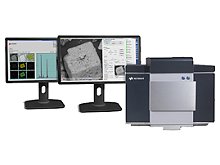
DESCRIBEThe remarkably compact Keysight 8500B field-emission scanning electron microscope (FE-SEM) has been optimized for low-voltage imaging, extremely high surface contrast, and resolution. This innovative, technologically advanced system also offers fully integrated energy dispersive spectroscopy (EDS) capabilities, allowing quantitative elemental analysis to be performed on arbitrary points, on a continuous line scan, or in a user-defined regional map. It can detect elements as light as carbon, up to americium. The easy-to-install, plug-and-play 8500B has been designed for use in practically any lab and requires only an AC power outlet. The novel, scientific-grade system offers several low-voltage imaging techniques that enhance surface contrast and permit nanoscale features to be observed on a wide variety of nanostructured materials, including polymers, thin films, biomaterials, and other energy-sensitive samples on any substrate, even glass.
|